
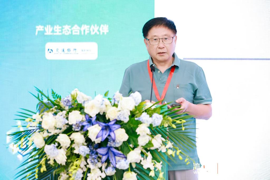
Professor Lin Fujiang from the Asia Pacific Science and Technology Association (Singapore) Proposes a Next-Generation, Ultra-High-Density Optical Interconnect Chip Roadmap, Introducing an “Eastern Taiji” Concept of Integrated Optoelectronic and Terrestrial-Aerospace Connectivity
新加坡亚太科学技术协会(APSTA)林福江教授分享下一代超高密度光互连芯片路径,提出“光电融合、天地融合”的东方太极式互联构想
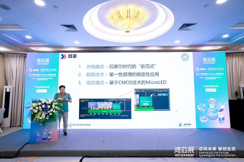
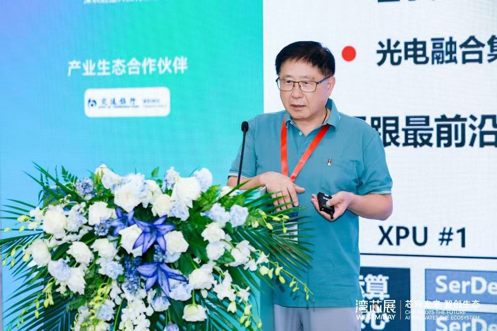
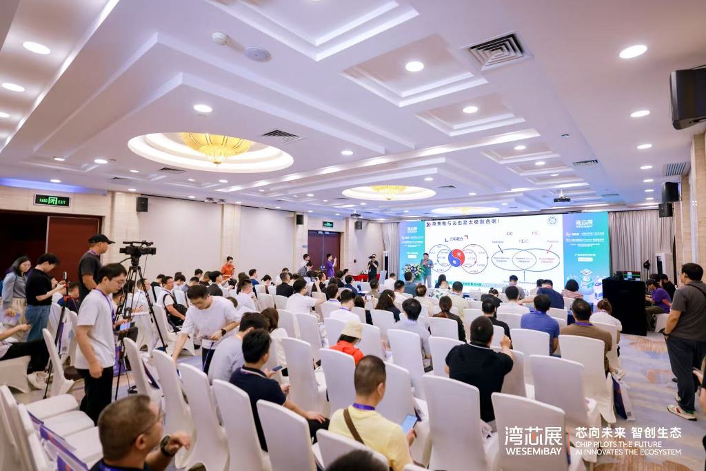
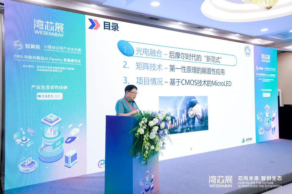
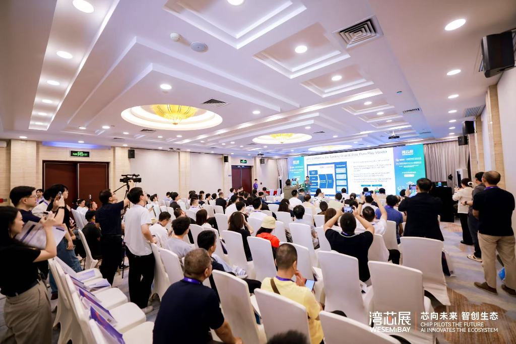
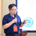
The 2026 Greater Bay Area Semiconductor Industry Ecosystem Expo recently took place, drawing significant industry attention. During the event, Professor Lin from the Asia-Pacific Science and Technology Association (Singapore) delivered a keynote speech titled “Next-Generation Ultra-High-Density Optical Interconnect SoC Chip Solution Based on Parallel-Matrix MicroLED Technology.” The presentation focused on the transformation of computing infrastructure driven by AI, systematically addressing the practical constraints—density, bandwidth, and power consumption—facing data center interconnects. Professor Lin introduced a novel approach to optical interconnect SoCs centered on parallel-matrix MicroLEDs, a concept that resonated strongly with the audience and drew enthusiastic applause.
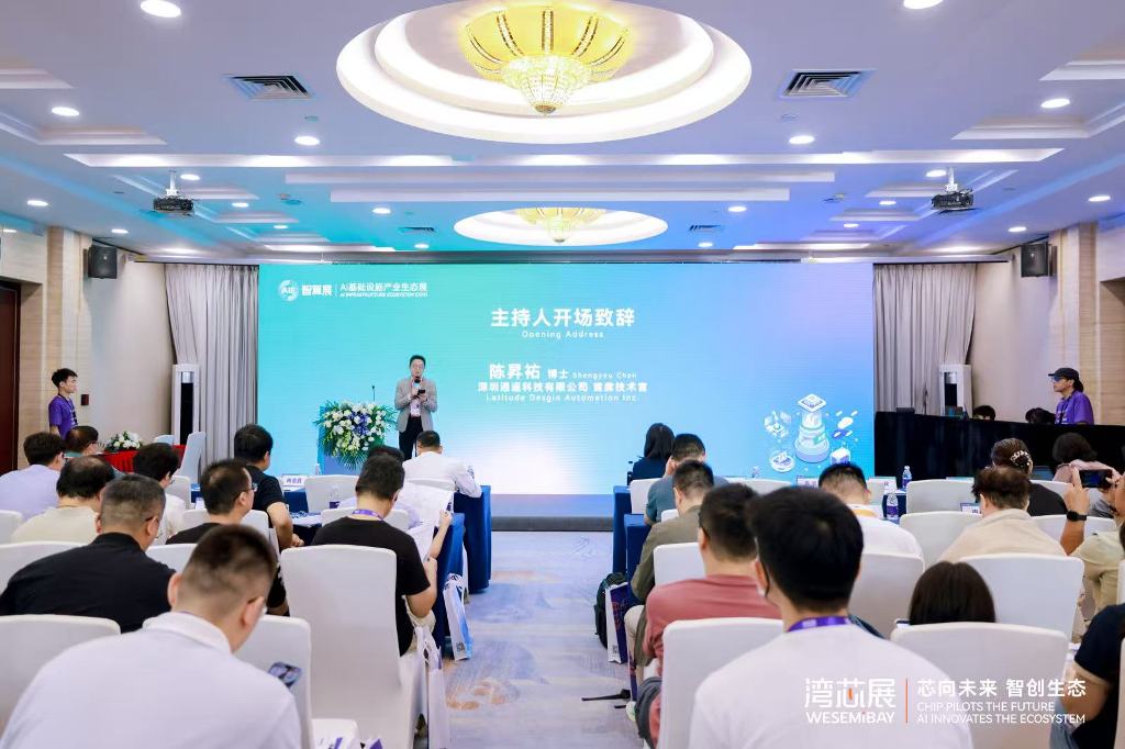
近日,2026 湾区半导体产业生态博览会在行业瞩目中举行。会上,来自新加坡亚太科学技术协会(Asia Pacific Science and Technology Association)的林教授发表主题演讲,题目为《基于并行矩阵 MicroLED 技术的下一代超高密度光互连 SoC 芯片解决方案》。演讲聚焦 AI 驱动下的算力基础设施变革,系统阐述了数据中心互连在密度、带宽与功耗上的现实约束,并提出以并行矩阵 MicroLED 为核心的光互连 SoC 新思路,现场反响热烈,获得全场听众热烈掌声。
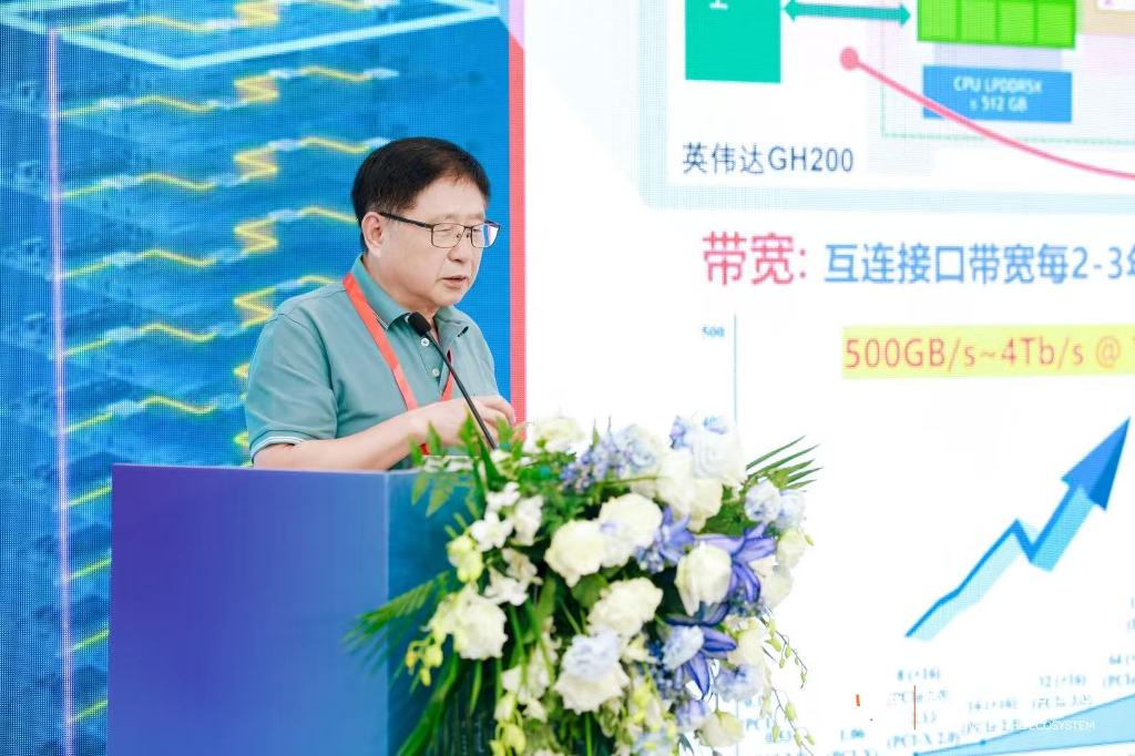
In his address, Professor Lin noted that AI and next-generation information technologies are fueling a new wave of technological upgrades and disruptive revolutions, with computing paradigms, packaging methods, and interconnect architectures evolving in tandem. Meanwhile, the development of high-performance computing (HPC) platforms, high-bandwidth memory (HBM), and data center systems is confronting a “triple-wall” bottleneck: higher integration demands shorter interconnects and greater I/O density; the training and inference of increasingly large models require wider link bandwidth; and the pressures of energy consumption and thermal management continue to drive up system costs. As the marginal returns of traditional electrical interconnects diminish in high-end computing scenarios, the industry is increasingly reaching a consensus on the shift from copper to optical interconnects (“replacing copper with light”).
林教授在演讲中指出,AI 与新一代信息技术正在推动新一轮技术升级和颠覆性革命,计算范式、封装方式与互连架构同步演进。与此同时,HCP、HBM 以及数据中心系统的发展正面临“密度、带宽、功耗”三墙瓶颈:更高集成度要求更短互连与更高 I/O 密度,更大模型训练与推理呼唤更宽链路带宽,而能耗与散热压力又持续抬升系统成本。传统电互连在高端算力场景中的边际收益递减,产业界对“光进铜退”的共识不断增强。
Against this backdrop, Professor Lin emphasized that photonic computing and optical interconnects have become an inevitable trend, accelerating the arrival of the “photonic era.” He suggested that future connectivity will no longer be confined to a single dimension—whether wired or wireless—but will instead emerge as a synergistic framework characterized by the integration of optoelectronics and the convergence of terrestrial and aerospace systems. This vision calls for seamless, low-latency, highly reliable, and energy-efficient connectivity spanning ground-based data centers, edge nodes, aerospace links, and end-user devices. He aptly characterizes this integration approach as “Oriental Taiji”—a dynamic equilibrium where rigid computational demands and flexible optical interconnect capabilities interact to unlock system-level performance.
在此背景下,林教授强调光子计算与光互连正成为确定性趋势,带动光子时代加速到来。他表示,未来互联不再局限于有线或无线单一维度,而是在天地融合、光电融合的大框架下形成协同:地面数据中心、边缘节点、空天链路以及终端设备之间,需要低时延、高可靠、高能效的一体化连接。他将这一融合路径形象地概括为“东方太极”——刚性的算力需求与柔性的光互连能力相互作用,在动态平衡中释放系统级性能。
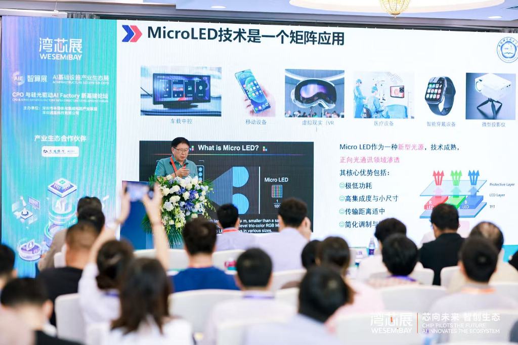
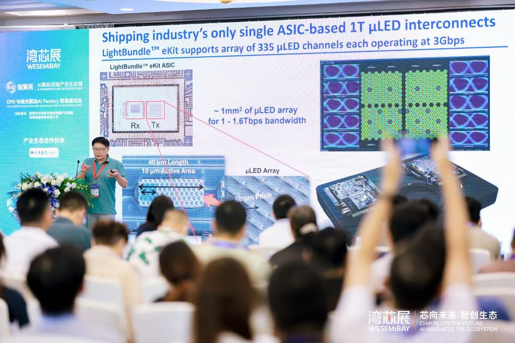
Professor Lin emphasizes that CMOS remains the foundational bedrock for large-scale manufacturing, cost control, and industrial ecosystem synergy. Building upon this, he proposes a novel concept for optical interconnect SoCs centered on “parallel-matrix CMOS MicroLEDs” based on SOI-CIS (Silicon-on-Insulator CMOS Image Sensor) technology. This approach leverages mature CMOS processes for high-density integration and drive control, utilizes SOI-CIS capabilities to enhance optoelectronic interfaces and array coordination, and employs parallel-matrix MicroLEDs to boost link bandwidth density and energy efficiency.
林教授特别强调,CMOS 仍是实现规模化制造、成本可控与产业生态协同的底座;在此基础上,他提出基于 SOI-CIS 的并行矩阵 CMOS MicroLED 为核心的光互连 SoC 新思路,即以成熟 CMOS 工艺承接高密度集成与驱动控制,以 SOI-CIS 相关能力增强光电接口与阵列协同,再通过并行矩阵 MicroLED 提升链路带宽密度与能效表现。
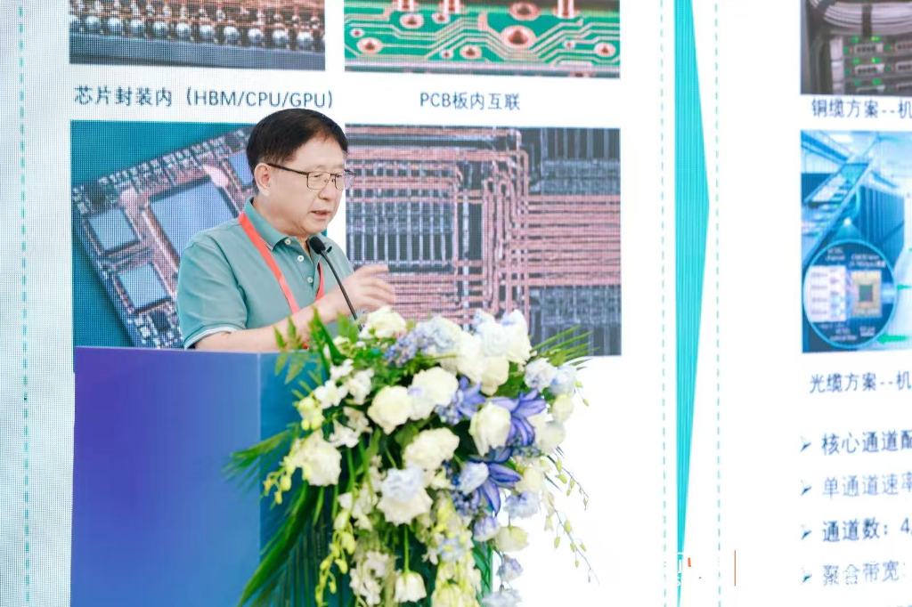
Focusing on key enabling technologies, Professor Lin highlights the SOI-CIS-CMOS-MicroLED technology stack. He argues that silicon-based platforms can be deeply integrated with mature CMOS processes; the structural and sensing/array capabilities of SOI-CIS, the high brightness and high modulation bandwidth of MicroLEDs, and the scalability afforded by the parallel-matrix architecture will collectively drive the engineering and industrialization of ultra-high-density optical interconnect SoCs. This solution promises to balance bandwidth density, energy efficiency, and cost-effectiveness across various scenarios—ranging from short-reach chip-to-chip and board-level interconnects to intra-rack, inter-rack, and even broader integrated space-ground connectivity—serving as a disruptive, accelerating technology to overcome the “three walls” (bottlenecks).
围绕关键使能技术,林教授重点介绍了 SOI-CIS-CMOS-MicroLED 技术组合。他认为,硅基平台可与成熟 CMOS 工艺深度协同,SOI-CIS 相关结构与感知/阵列能力、MicroLED 的高亮度与高调制带宽特性,以及并行矩阵架构带来的可扩展性,将共同推动超高密度光互连 SoC 走向工程化与产业化。该方案有望在短距 chip-to-chip、板级互联、机柜内与机柜间链路,乃至更广义的天地一体化互联场景中,兼顾带宽密度、能效比与成本曲线,成为破解“三墙”瓶颈的颠覆性加速技术。
In his concluding remarks, Professor Lin called for collaborative innovation across the entire industrial chain—encompassing materials, devices, packaging, drive circuitry, algorithms, and standards—to transform isolated performance breakthroughs into system-level competitiveness. Attendees noted that the presentation offered both a clear-eyed assessment of existing bottlenecks and a viable technical roadmap for next-generation computing infrastructure, providing a fresh agenda for collaboration within the Greater Bay Area’s semiconductor ecosystem—specifically regarding advanced packaging, optoelectronic integration, and AI-driven computational interconnects.
演讲最后,林教授呼吁产业链上下游围绕材料、器件、封装、驱动、算法与标准协同创新,把单点性能突破转化为系统级竞争力。现场多位参会人士表示,该演讲既有对瓶颈的清醒判断,也给出了面向下一代算力基础设施的可实施技术路线,为湾区半导体生态围绕先进封装、光电子集成与 AI 算力互联的合作提供了新议题。



Leave a Reply