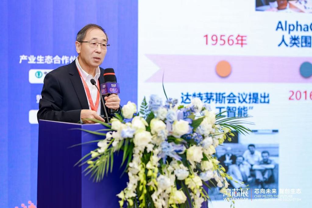
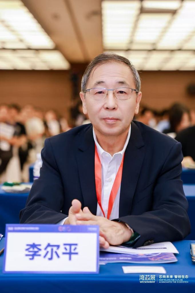
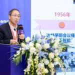
The “International Forum on Advanced Packaging Processes and Materials,” held in conjunction with the 3rd Integrated Circuit Materials Industry Development Forum—part of the 2026 Greater Bay Area Semiconductor Ecosystem Expo—opened today. During the event, Er-Ping Li, a Qiushi Chair Professor at Zhejiang University, Foreign Member of the Chinese Academy of Engineering, and Fellow of the Academy of Engineering, Singapore, delivered a keynote speech titled “AI-Empowered Integrated Circuits: A New Engine for the Post-Moore Era.” He provided an in-depth exploration of the synergistic evolution and mutual empowerment between artificial intelligence and integrated circuits, a topic that resonated strongly with the attendees.
2026湾区半导体生态博览会系列活动之一——”国际先进封装工艺与材料论坛暨第三届集成电路材料产业发展论坛”于今日隆重召开。会上,浙江大学求是讲席教授、中国工程院外籍院士、新加坡工程院院士李尔平以《AI赋能集成电路:后摩尔时代的新引擎》为题发表主旨演讲,深入阐述了人工智能与集成电路双向赋能、协同演进的技术图景,引发与会嘉宾的热烈反响。
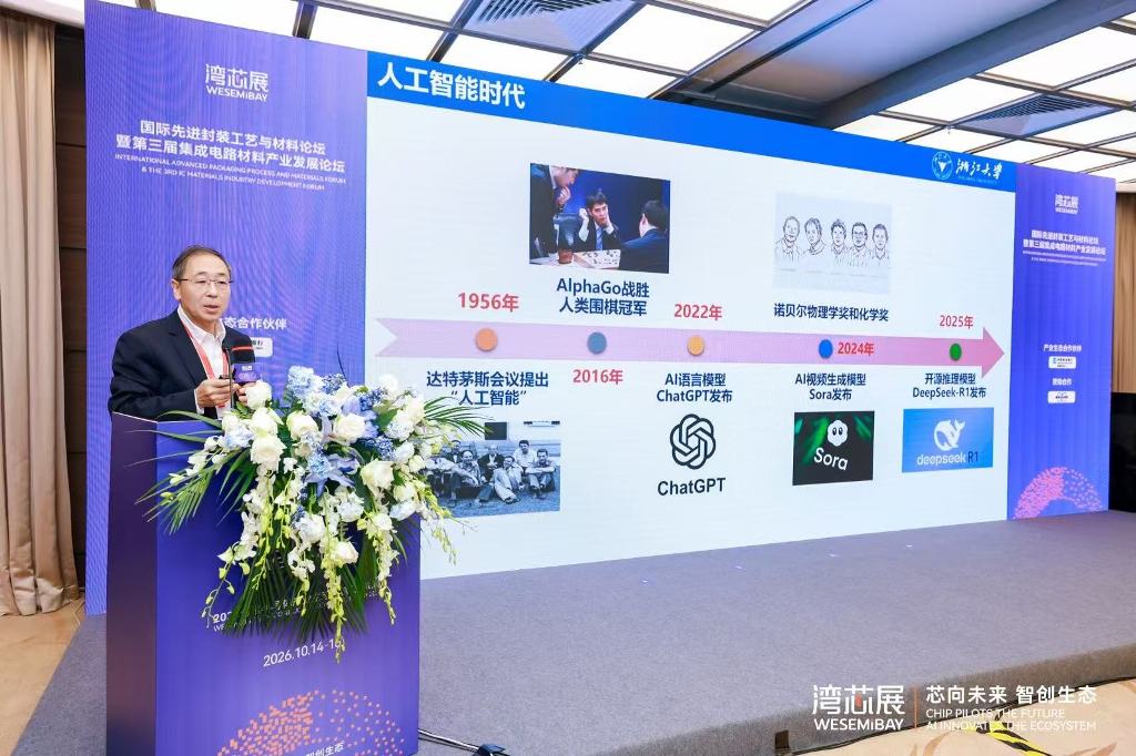
In his presentation, Academician Li noted that as Moore’s Law approaches its physical limits, the traditional path of enhancing chip performance solely through process scaling is narrowing. The integration of artificial intelligence, however, has opened up entirely new avenues for growth within the integrated circuit (IC) industry. “AI is reshaping the IC industry across the entire value chain—from design and manufacturing to testing—emerging as one of the most critical technological pathways in the post-Moore era.”
李尔平院士在报告中指出,随着摩尔定律逼近物理极限,单纯依靠制程微缩提升芯片性能的道路日益收窄,人工智能的引入为集成电路产业打开了全新的增长空间。”AI正在从设计、制造到测试的全链条重塑集成电路产业,成为后摩尔时代最关键的技术路径之一。”
Design: AI Drives the Intelligent Transformation of EDA
In the design phase, artificial intelligence has deeply permeated every stage of chip development. Li explained that AI algorithms can significantly optimize processes such as placement and routing, logic synthesis, and functional verification, thereby drastically shortening design cycles and reducing costs. “Design iterations that once took engineers weeks to complete can now be finished in a matter of hours with the help of AI-assisted tools—a capability of immense value for products requiring rapid iteration.”
He particularly highlighted the groundbreaking application of large-scale models and reinforcement learning in the field of Electronic Design Automation (EDA). By combining the comprehension capabilities of large language models with the decision-making prowess of reinforcement learning, EDA tools are undergoing a qualitative leap—evolving from mere “auxiliary tools” into “intelligent design partners.” This transformation simultaneously lowers the barriers to entry for chip design while enhancing overall efficiency.
设计端:AI驱动EDA智能化跃迁
在设计环节,人工智能技术已深度渗透芯片设计的各个环节。李尔平介绍,AI算法能够显著优化布局布线、逻辑综合与功能验证流程,大幅缩短设计周期、降低设计成本。”过去需要工程师数周完成的设计迭代,借助AI辅助工具可在数小时内完成,这对于快速迭代的产品而言意义重大。”
他特别强调了大模型与强化学习技术在EDA(电子设计自动化)领域的突破性应用。通过将大语言模型的理解能力与强化学习的决策能力相结合,EDA工具的自动化水平正在实现质的飞跃,从”辅助工具”向”智能设计伙伴”转变,使芯片设计的门槛与效率迎来双重改善。
Manufacturing and Testing: Machine Learning as a Safeguard for Yield
In the realms of manufacturing and testing, machine learning has also demonstrated significant power. Li pointed out that yield prediction, defect detection, and process control represent the most mature and deeply integrated applications of machine learning in these areas today. A high-precision defect detection system based on deep learning can rapidly identify nanoscale defects during the wafer manufacturing process, while process control models enable real-time parameter optimization, minimizing yield fluctuations.
“As a vital pathway for extending Moore’s Law, advanced packaging—with its complex, heterogeneous integration—poses unprecedented challenges for process control. This is precisely where AI can truly excel,” noted Li Erping. He emphasized that AI-driven optimization of advanced packaging processes is becoming a key lever for overcoming performance bottlenecks.
制造与测试端:机器学习守护良率生命线
在制造与测试环节,机器学习同样展现出强大威力。李尔平指出,良率预测、缺陷检测与工艺控制是机器学习当前最成熟、应用最深入的场景。基于深度学习的高精度缺陷检测系统,能够在晶圆制造过程中快速识别纳米级缺陷;工艺控制模型则可实时优化参数,将良率波动降至最低。
“先进封装作为延续摩尔定律的重要路径,其复杂的异构集成结构对工艺控制提出了前所未有的挑战,而这恰恰是AI大显身手的舞台。”李尔平表示,AI赋能的先进封装工艺优化,正在成为突破性能瓶颈的关键抓手。
A Mutually Reinforcing Journey: The Co-evolution of AI and Chips
Li Erping further elaborated on his profound insight into the “mutually reinforcing” relationship between AI and chips: on one hand, AI provides intelligent tools for chip design and manufacturing; on the other, the demand for high-performance, low-power AI chips drives the evolution of integrated circuits toward greater computational power, higher energy efficiency, and increased intelligence. “Advanced packaging and material innovations provide the physical foundation for AI chips, while AI algorithms serve as an intelligent engine for packaging design and material selection—the two empower each other, driving a continuous, upward spiral of advancement.”
He argued that in the “post-Moore” era, the development logic of the integrated circuit industry has shifted from “isolated breakthroughs” to “systemic synergy.” The deep integration of design, manufacturing, packaging, and materials—augmented by AI across the entire value chain—will define a new paradigm for industrial competition.
双向奔赴:AI与芯片的协同进化
李尔平进一步阐述了他对”AI与芯片双向促进”关系的深刻理解:一方面,AI为芯片设计制造提供智能化工具;另一方面,高性能、低功耗的AI芯片需求,也在牵引集成电路向更高算力、更低能耗、更智能化的方向演进。”先进封装与材料创新为AI芯片提供物理载体,AI算法则为封装设计、材料筛选提供智能引擎,二者相互成就、螺旋上升。”
他认为,在后摩尔时代,集成电路产业的发展逻辑已从”单点突破”转向”系统协同”——设计、制造、封装、材料的深度融合,加上AI的全链条赋能,将共同构成产业竞争的新范式。
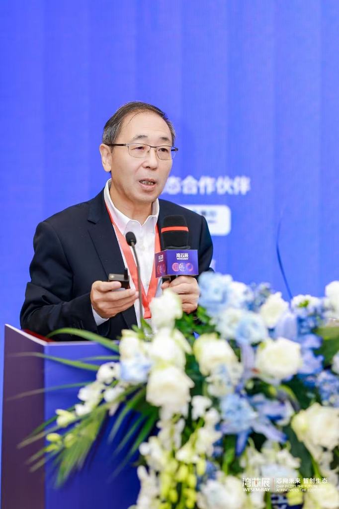
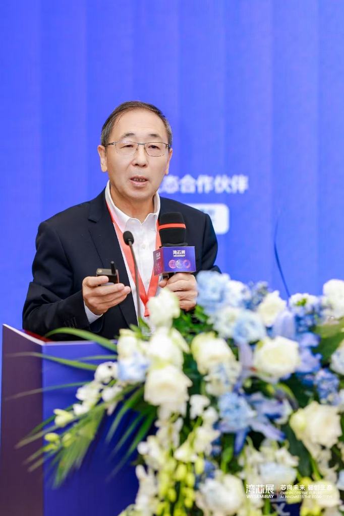
In his concluding remarks, Li Erping called for enhanced collaborative innovation across the entire industrial chain to foster a deeper integration of AI technology and the integrated circuit sector. “Those who can seize the initiative in this two-way empowerment between AI and chips will hold the key to shaping the future of the industry in the post-Moore era.”
演讲最后,李尔平呼吁产业链上下游加强协同创新,推动AI技术与集成电路产业更深层次的融合。”谁能在AI与芯片的双向赋能中占据先机,谁就能在后摩尔时代掌握产业发展的主动权。”
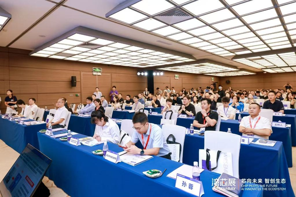
The presentation was attended by hundreds of representatives from global semiconductor companies and research institutions, drawing a full house and sparking a vibrant exchange of ideas. Experts in attendance noted that the insights shared by Academician Li Erping provided a clear direction for the industry, offering fresh perspectives and pathways for technological innovation within the advanced packaging and materials sector.
来自全球半导体企业、科研院所的数百位与会代表聆听了本次报告,现场座无虚席、交流气氛热烈。与会专家表示,李尔平院士的报告为行业指明了方向,也为先进封装与材料产业的技术创新提供了新的思路与路径。
Leave a Reply