
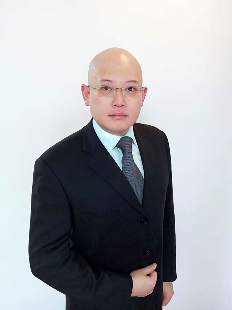
SrMIEEE PMP
Experience
- VP and GM at JCET Group / Technology Service Business Unit (Shanghai), 06/2022 – present
- Chief Architect at HuaWei Hisilicon Chip System Platform (Shanghai), 06/2017 – 05/2022
- Manager and Principal Engineer at Intel Foundry / IoT Group (Portland), 10/2014 – 05/2017 (7.5-year)
- Package SI/PI Tech Lead at Intel Tech Manufacturing Group (California), 06/2010-05/2013 (3-year)
- Visiting Researcher at IBM New York T.J. Watson Research Center, 09/2009-12/2009 (4-month)
- Lecturer of EE480 Microwave Eng. EE579 Computation EM at U. of Washington, 09/2008-03/2009 (6-month)
Certification
PMP, Project Management Project Management Institute at Stanford, 11/2012 Proficiency
Education
- Ph.D. in Electrical Engineering, University of Washington, 06/2010 Distinguished; Dissertation: Fast electromagnetic modeling of high speed interconnects in advanced electronic packaging
- M.S. in Electrical Engineering, U. of Washington in Seattle, 12/2007 GPA 3.80; Projects: Low-noise RF amplifier design, dual-band antenna design, charge-pumped PLL design and validation
- B.Eng. Electronic Commu. Eng., City Univ. of Hong Kong, 10/2005 GPA 3.91 First Class; Dean’s Highest Honor, 3-year full scholarship for top Chinese undergraduates by HK Jockey Club
- Elite Program in Computer Science, Shanghai Jiao Tong Univ., 06/2002 Summa Cum Laude
Achievements
- Patents 20+,
- Publications 60+,
- Total citations 700+,
- Influence G-index 26,
- H-index 15, I-10: 20
Representative Journal Papers
- [J16] S. Huang, B. Lee, B. Wu, K. Xiao, X. Ye, “Absorbing termination for high-frequency measurements of interconnects,” IEEE CPMT. 2017. [cite by 4]
- [J15] B. Wu and H. L. Lo, “Methods and designs for improving the signal integrity of vertical interconnects in high performance packaging,” PIER. 2012. [cite by 25]
- [J14] B. Wu, B. Brown and E. Warner, “High density interconnect board design for wafer level packaging,” IET Electronics Lett., 2011. [cited by 13]
- [J13] B. Wu, X. Gu, L. Tsang, and M. B. Ritter, “Electromagnetic modeling of massively coupled through silicon vias for 3-D interconnects,” MOTL. 2011. [cited by 32]
- [J12] B. Wu and L. Tsang, “Full-wave modeling of multiple vias using differential signaling and shared antipad in multilayered high speed vertical interconnects,” PIER. 2009. [cited by 45]
- [J10] B. Wu and L. Tsang, “Signal integrity analysis of package and printed circuit board with multiple vias in substrate of layered dielectrics,” IEEE Trans. Adv. Packag., 2010. [cited by 57]
- [J9] D.G. Kam, et.al., and B. Wu, “Is 25 Gb/s on-board signaling viable?” invited special issue, IEEE Trans. Adv. Packag., 2009. [cited by 99]
- [J8] B. Wu and L. Tsang, “Modeling multiple vias with arbitrary shape of antipads and pads in high speed interconnect circuits,” IEEE MWCL. 2009. [cited by 53]
- [J6] B. Wu and L. Tsang, “Fast computation of layered medium Green’s functions of multilayers and lossy media using fast all modes method and numerical modified steepest-descent path method,” IEEE Trans. Microw. Theory Tech. 2008. [cited by 43]