Conference Overview | 会议概览
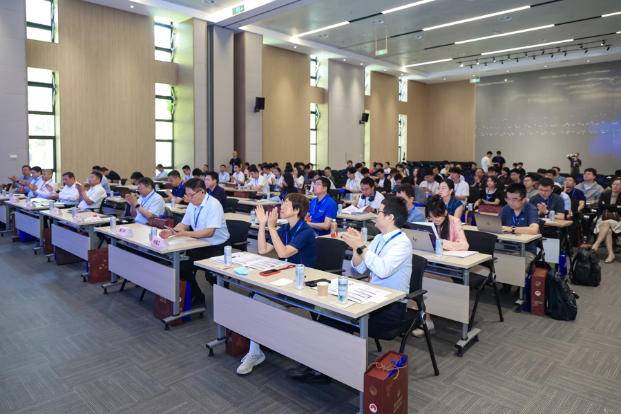
The 10th China MOS-AK International Conference on Device Modeling—meticulously organized by the Device Modeling Professional Committee (Preparatory) of the China Semiconductor Industry Association, the Yangtze River Delta Integrated Circuit Industrial Application Technology Innovation Center, and the IEEE Nanjing Section, and hosted by the School of Integrated Circuits at Southeast University and the Asia-Pacific Science and Technology Association (APSTA)—concluded successfully on August 27–28, 2026, at the Wuxi Campus of Southeast University.
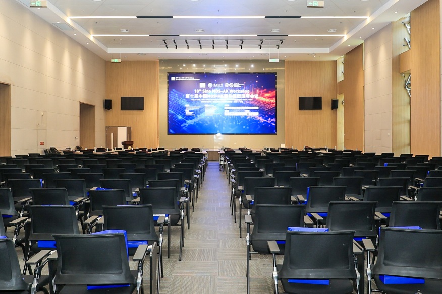
由中国半导体行业协会器件建模专业分会(筹)、长三角集成电路工业应用技术创新中心、IEEE Nanjing Section的精心策划,东南大学集成电路学院、亚太科学技术协会(APSTA)承办的“第十届中国MOS-AK器件模型国际会议”于2026年8月27日至28日在东南大学无锡校区圆满落幕。
Centered on the theme “AI-Empowered Device Modeling,” this academic event achieved fruitful results and garnered widespread acclaim.
这场以“AI赋能器件建模”为主题的学术盛会,取得了丰硕成果与广泛好评。
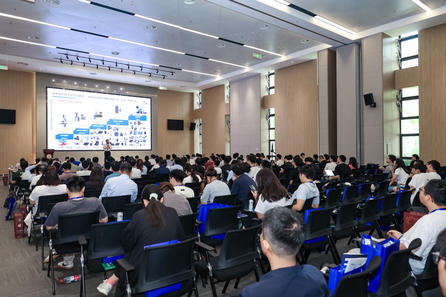
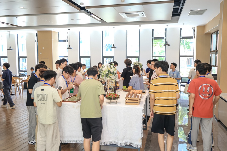
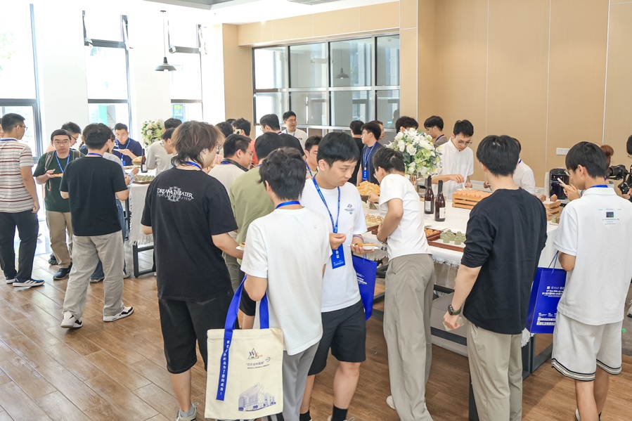
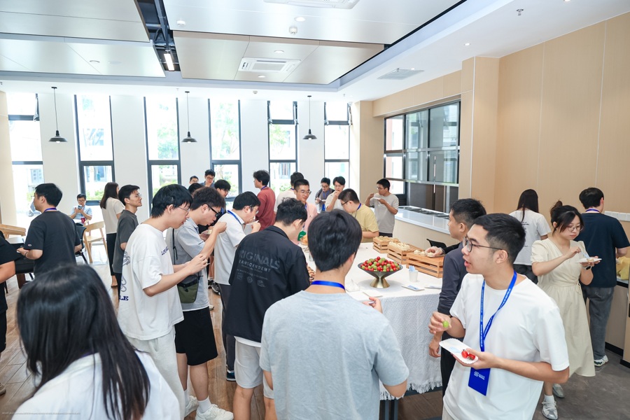
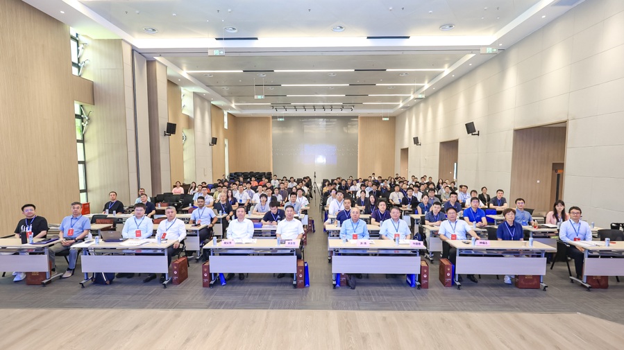
The conference brought together top experts from domestic universities, wafer foundries, and the EDA, packaging/testing, and equipment sectors. It established a high-quality platform for dialogue and deep integration among industry, academia, and research, catering to corporate modeling engineers, university faculty and students, and technical professionals. The two-day agenda featured an opening ceremony, keynote speeches, thematic presentations, five specialized breakout sessions, roundtable discussions, technical training, and networking events.
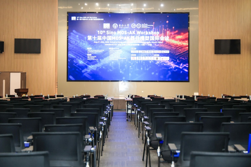
大会汇聚了来自国内高校、晶圆厂、EDA、封测及设备领域的顶尖专家,面向企业模型工程师、高校师生和行业技术人员,搭建起一座产学研深度融合的高质量对话平台。在为期两天的议程中,开幕式、主旨报告、主题报告、五大专题分论坛、圆桌研讨、技术培训及晚宴交流等环节依次展开。
Experts delivered insightful and cutting-edge presentations covering the entire technology chain—including device characterization, compact modeling, parameter extraction, model libraries, and open-source PDKs, as well as silicon photonics, advanced packaging, wide-bandgap semiconductors, emerging memory technologies, and quantum devices. Ideas from diverse fields converged and sparked dynamic exchanges, giving rise to a constant stream of new perspectives and approaches; this fostered cross-disciplinary inspiration and intellectual synergy, injecting powerful momentum into the future development of device modeling technology.
嘉宾们围绕器件表征、紧凑模型、参数提取、模型库、开源PDK,以及硅光、先进封装、宽禁带、新型存储与量子器件等全链条技术,奉献了一场场视角独到、内容前沿的精彩演讲。不同领域的思想在此激荡交锋,新观点、新思路层出不穷,真正实现了跨界启迪与智慧共振,为器件建模技术的未来发展注入了强劲动能。

Main Forum | 主论坛
Standing at the Industry’s Strategic High Ground—Gaining Insights into New Paradigms for Device Modeling | 站在产业制高点,洞见器件建模新范式
Held on August 27–28, the main forum brought together academicians and leading industry experts; through a series of high-profile keynote and thematic presentations, they outlined a top-level blueprint for the device modeling industry.
8月27日至28日主论坛汇集院士、产业领军专家,多场重磅主旨与主题报告,勾勒器件建模产业顶层蓝图。
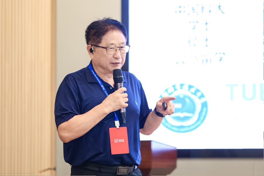
Lin Fujiang (University of Science and Technology of China) | 林福江(中国科学技术大学)
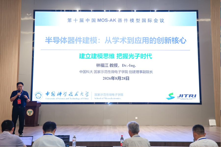
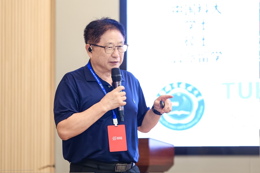
In his presentation titled “Semiconductor Device Modeling: The Core of Innovation from Academia to Application,” Lin Fujiang (University of Science and Technology of China):
- Emphasized the importance of a modeling mindset, noting that modeling focuses on prediction rather than mere data fitting and that model parameters are more critical than the model itself; outlined key practical points for device parameter extraction; discussed small-signal models and photonic integration; and advocated for the rational application of AI combined with physical principles.
林福江(中国科学技术大学) 在 《半导体器件建模是学术到应用的创新核心》 的演讲中:
- 强调建模思维的重要性,建模重在预测而非单纯数据拟合,模型参数比模型本身关键,讲解器件提参多项实操要点,还谈及小信号模型、光集成,主张结合物理原理合理运用 AI
Ye Tianchun (Institute of Microelectronics of the Chinese Academy of Sciences) | 叶甜春(中国科学院微电子研究所)
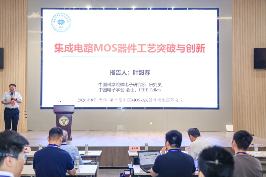
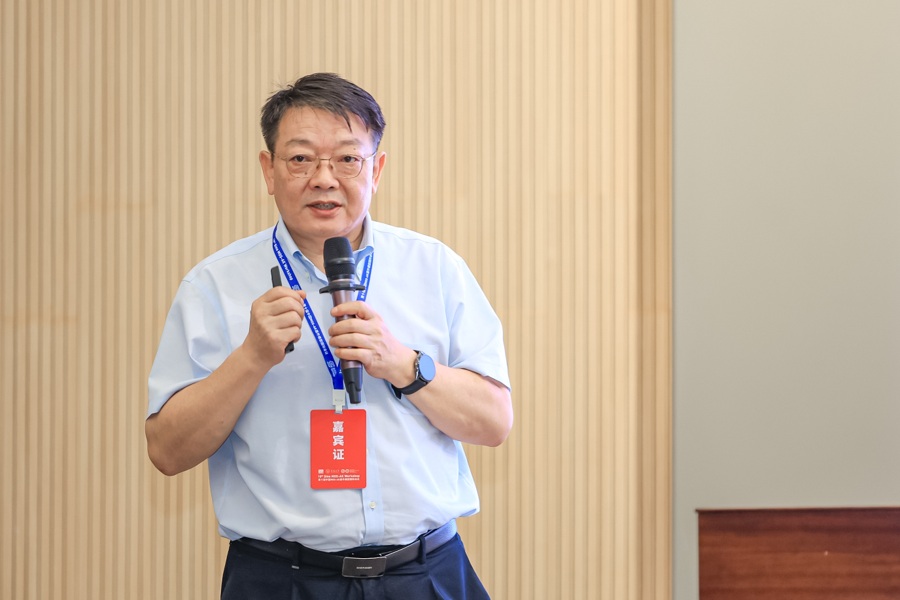
In his presentation titled “Breakthroughs and Innovations in Integrated Circuit Device Process Technology,” Ye Tianchun (Institute of Microelectronics of the Chinese Academy of Sciences) stated:
- my country’s integrated circuit sector urgently needs to break free from path dependency, open up new development tracks, establish a new industrial ecosystem, achieve independent development, and reshape the industrial system.
- MOS device process technology serves as a crucial foundation for advancing state-of-the-art integrated circuit manufacturing. Since 2009, the Institute of Microelectronics has conducted long-term pioneering R&D on process technologies for high-k metal gate CMOS, FinFET, and more advanced GAA devices across the 22nm, 14nm, and 3nm technology generations.
- These efforts have yielded a series of innovative achievements and established a systematic intellectual property protection framework. Key technologies have been applied to the advanced manufacturing processes and critical equipment of major domestic and international integrated circuit companies, generating significant economic and social benefits.
叶甜春(中国科学院微电子研究所) 在 《集成电路器件工艺突破创新》 的演讲中:
- 我国集成电路发展亟需摆脱路径依赖,开辟新赛道,形成产业新生态,实现自主发展并重塑产业体系
- MOS器件工艺技术是推动集成电路先进制造发展的重要基础,微电子所从2009年起,在22-14-3纳米技术代后高k金属栅CMOS、FinFET以及更先进的GAA器件工艺技术上展开了长期的先导研发。
- 取得一系列的创新成果,建立了系统的自主知识产权保护体系,关键技术在国内外集成电路重要企业的先进制造工艺和关键装备中得到应用,取得了显著的经济和社会效益。
Ma Yutao (Galileo Electronic Design, Shanghai) | 马玉涛(上海概伦电子)
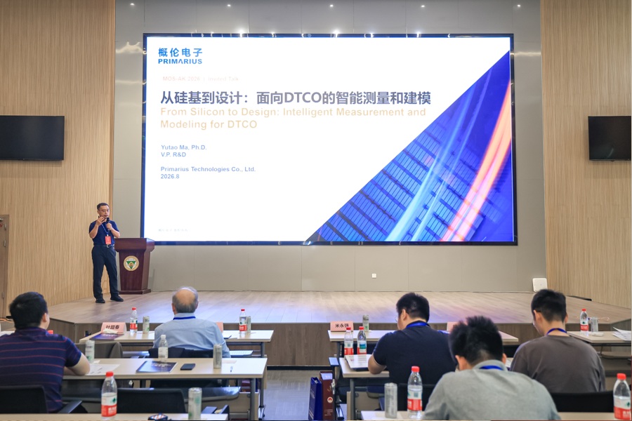
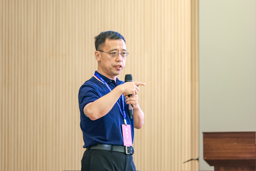
In the presentation “From Silicon to Design: Intelligent Measurement and Modeling for DTCO,” Ma Yutao (Galileo Electronic Design, Shanghai) stated:
- 1 Measurement defines what the model can know.
- 2 Compact models translate silicon behavior into design language.
- 3 Spec-driven extraction turns expert know-how into repeatable workflow
- 4 Al helps when constrained by physics, QA and lineage.
- 5 DTcO needs test + model + extraction + simulation as one learning loop.
马玉涛(上海概伦电子) 在 《从硅基到设计:面向DTCO的智能测量和建模》 的演讲中:
- 1 测量定义了模型可以知道的内容。
- 2 紧凑型模型将硅行为转化为设计语言。
- 3 规格驱动提取将专家专业知识转化为可重复的工作流程
- 4 当受到物理、QA和血统的限制时,人工智能会有所帮助。
- 5 DTcO需要测试+模型+提取+模拟作为一个学习循环。
Other Speakers | 其他演讲人
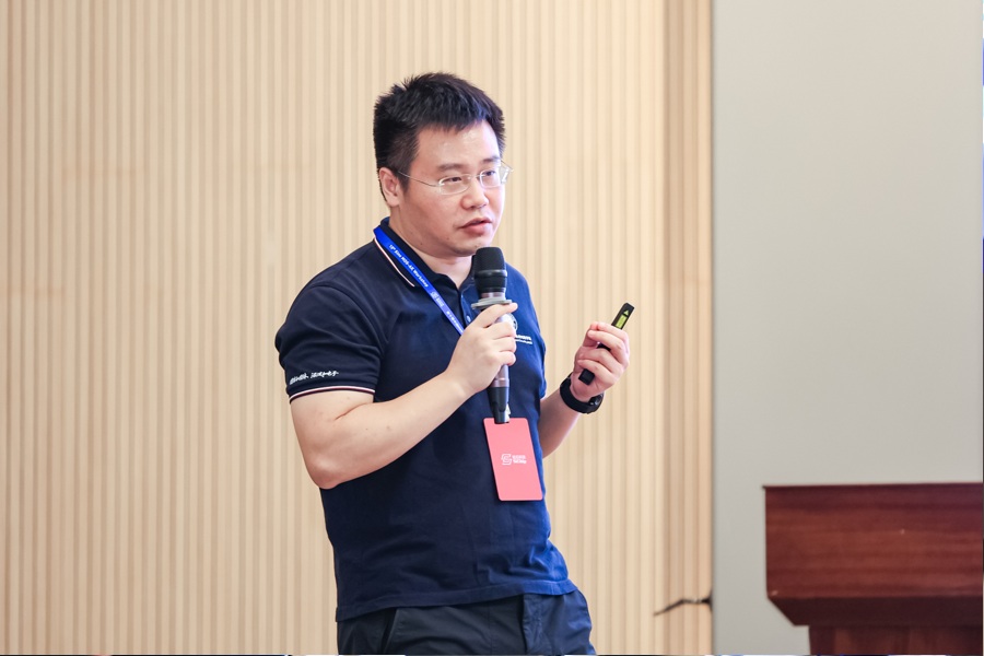
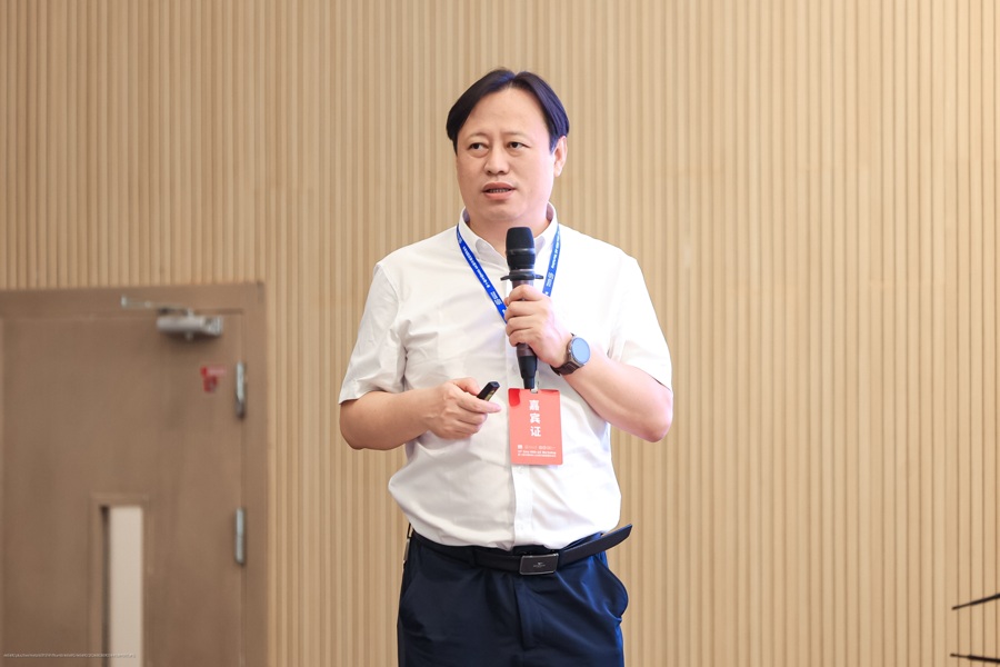
- 赵毅(珠海硅芯科技) 演讲《2.5D/3D IC AI+EDA重构先进封装系统设计工艺协同优化(STCO)新范式》
- 谭旻(华中科技大学) 演讲《光电融合紧凑建模基础问题与最新进展》
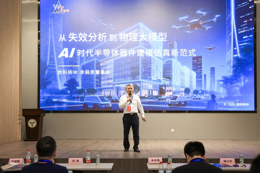
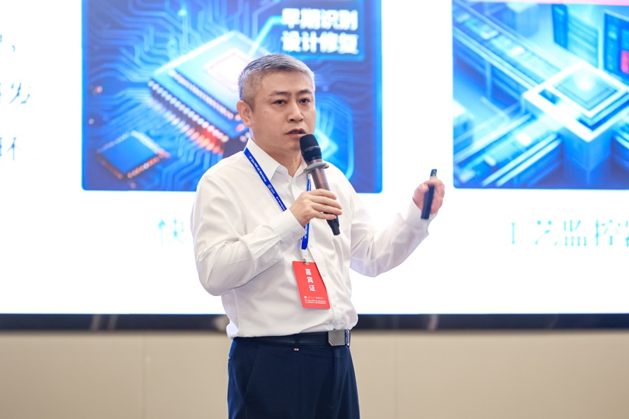
- 李晓旻(胜科纳米) 演讲《从”失效分析”到”物理大模型”:AI时代半导体器件建模仿真新范式》
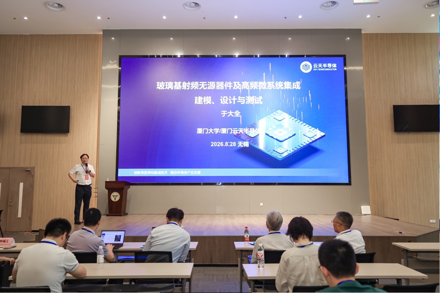
- 于大全(厦门大学/云天半导体) 演讲《玻璃基射频器件相关产业视角分享》
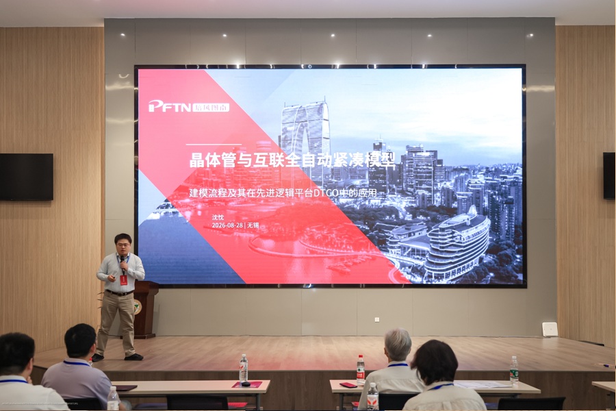
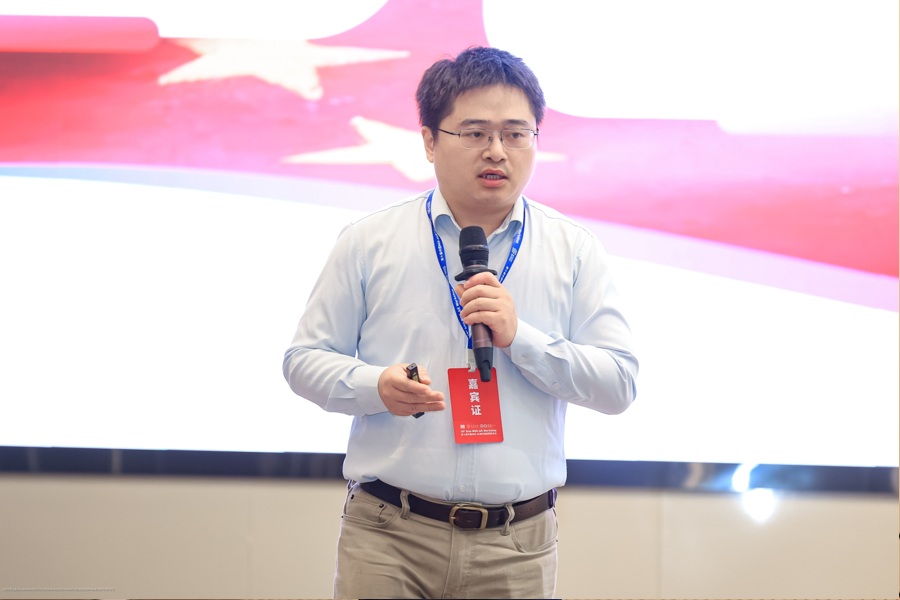
- 沈忱(上海培风图南半导体) 演讲《全自动紧凑建模流程相关产业视角分享》
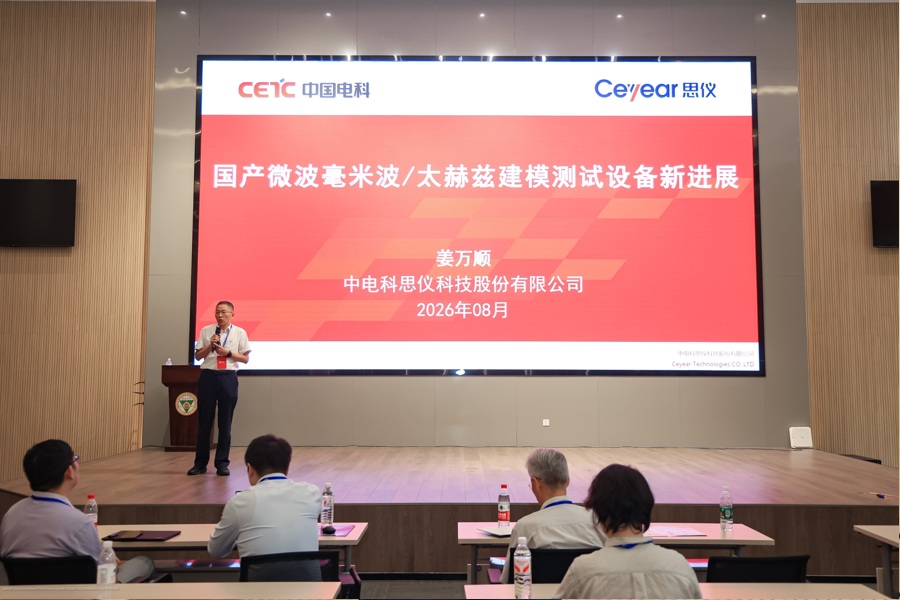
- 姜万顺(中电科思仪科技) 演讲《国产微波毫米波太赫兹测试设备相关产业视角分享》
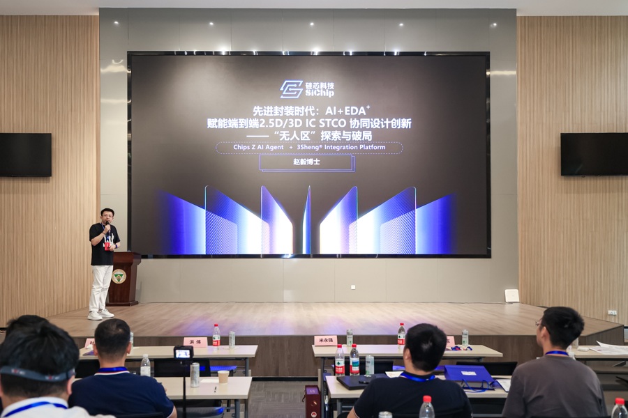
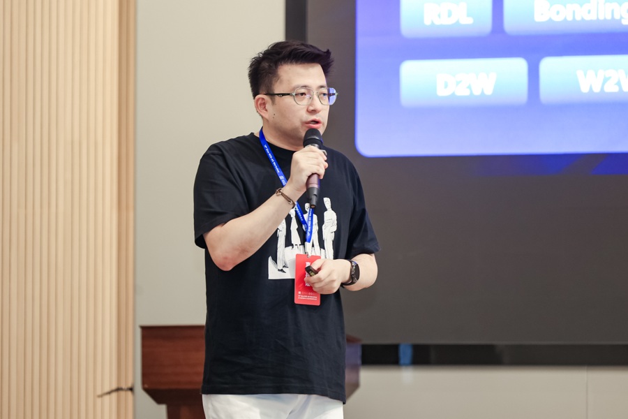
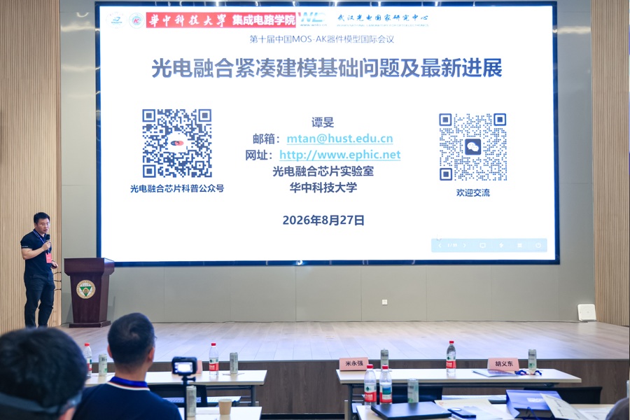
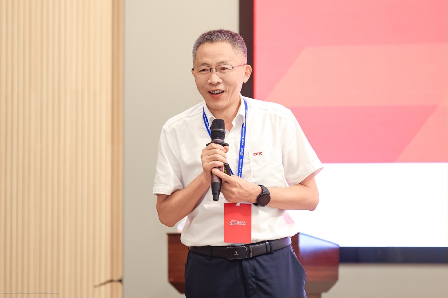
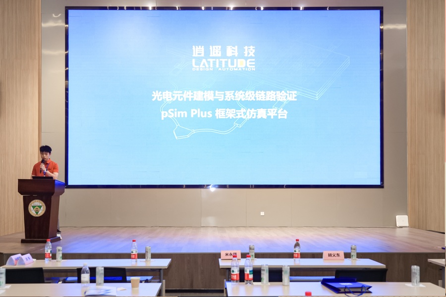
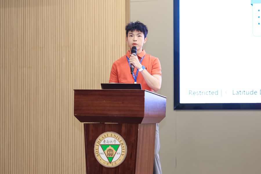
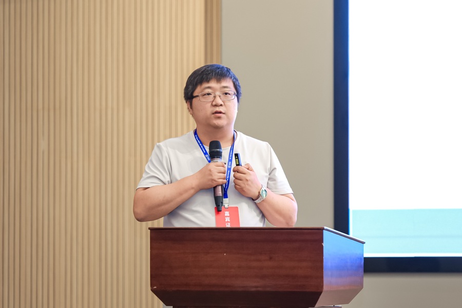
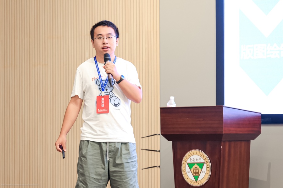
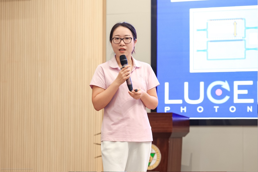
Topic 1: Compact Modeling and Co-simulation of Silicon Photonics, Optoelectronic Devices, and Photonic Interconnects in the AI Era | 专题一:AI时代下硅光技术、光电子器件、光子互连等的紧凑模型和联合仿真
论坛主席:谭旻、吴明辉
- 陳昇祐(上海逍遙光電) 演讲《光子运算系统层级光电融合模拟的Verilog实数建模》
- 赵昀松(上海曼光信息) 演讲《AI智能体落地硅光芯片设计的探索与进展》
- 马蔚(浙江大学) 演讲《算法驱动微纳光学逆向设计与工艺约束下的优化方法》
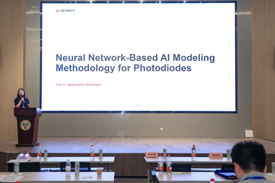
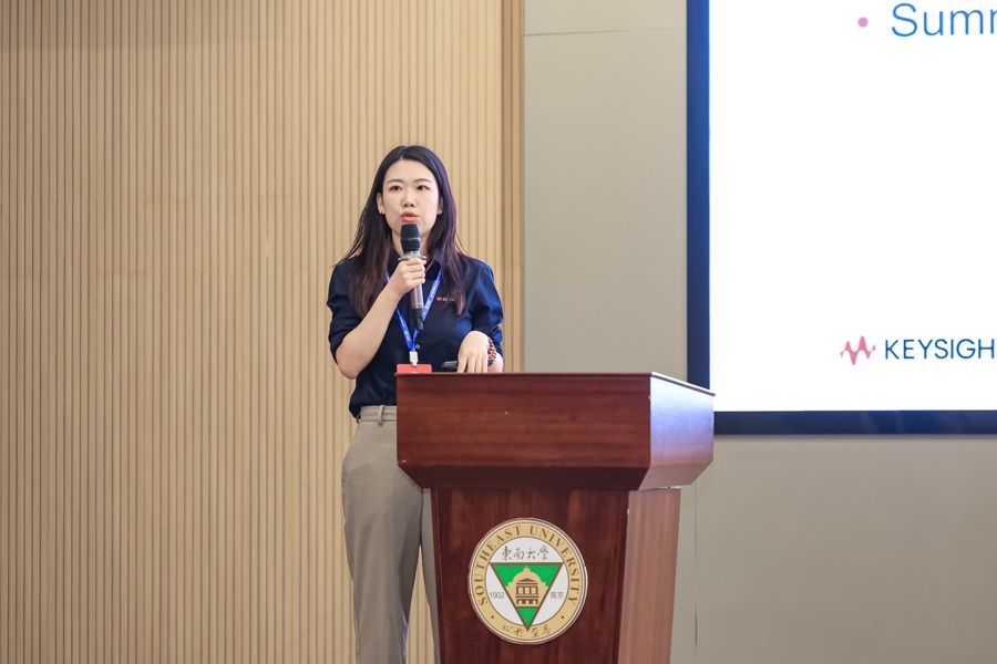
- 李依奥(Keysight是德科技) 演讲《基于物理模型与人工神经网络融合的光电二极管高精度建模方法》
- 王高峰(杭州电子科技大学) 演讲《面向光子互连的光电联合仿真与器件模型验证:SuperEM实践》
- 宋志刚(中国科学院半导体研究所) 演讲《基于华大九天珂晶达的光电子器件紧凑模型库》
- 曹如平(杭州广立微电子) 演讲《基于原生波域求解器的高效光电协同设计》
- 于飞(广东工业大学) 演讲《面向快速紧凑模型验证的通用参数提取工具》
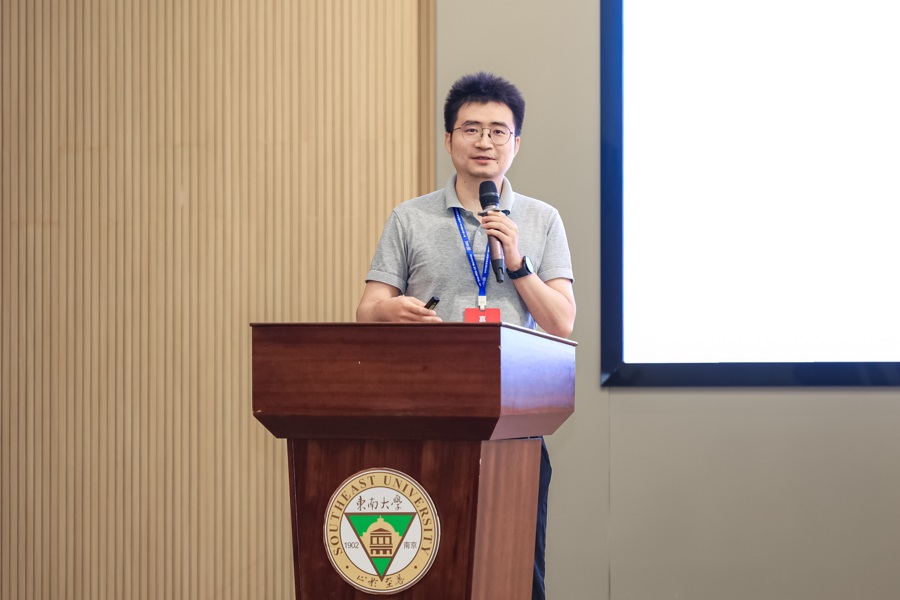
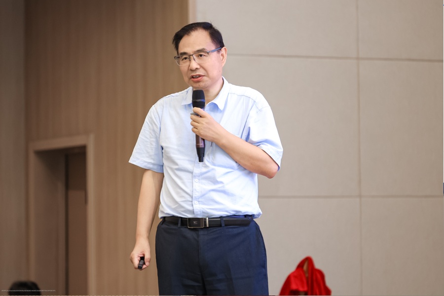
Topic 2: AI-Enabled Modeling and Simulation for Collaborative Innovation in 2.5D/3D Advanced Packaging | 专题二:2.5D/3D先进封装协同创新的AI助力建模和仿真
论坛主席:张硕、金文超
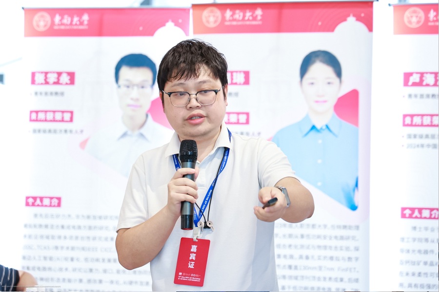
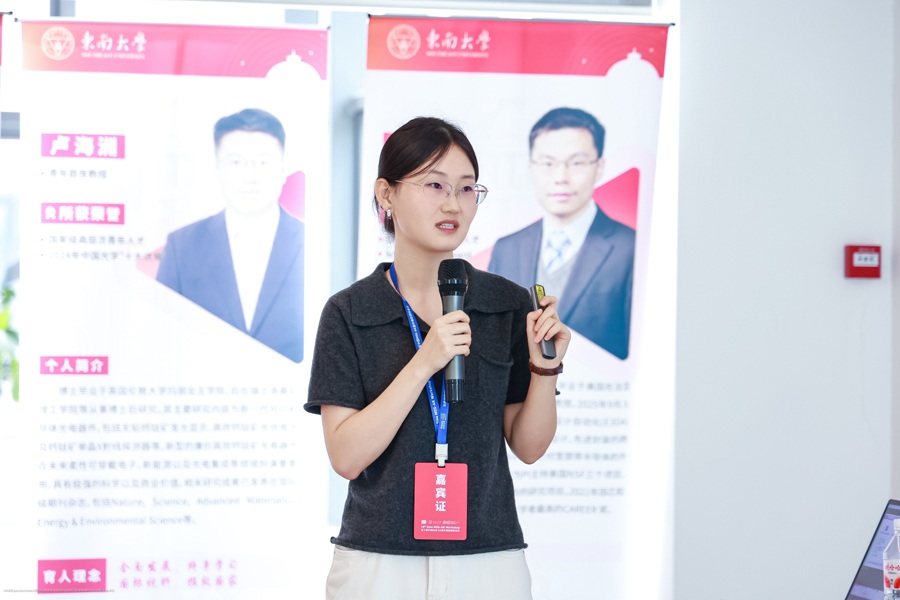
- 蒲菠(宁波德图科技)演讲《2.5D/3D先进封装互连技术协同建模与优化》
- 金洲(浙江大学)演讲《面向2.5D/3D先进封装的物理数据协同建模:从热仿真到热应力预测》
- 谢达(无锡中微亿芯)演讲《面向大容量高密度的2.5D异构芯粒技术研究》
- 王志昂(复旦大学)演讲《面向多范式三维集成统一开源物理实现平台的探索与实践》
- 温继敏(芯和半导体)演讲《面向2.5D/3D先进封装协同设计的AI辅助射频模组分层行为建模》
- 闵成彧(重庆联合微电子中心CUMEC)演讲《面向CPO的硅光有源TSV集成工艺与光电协同设计》
- 韩丽霞(南京航空航天大学)演讲《面向大模型推理的2.5D异构存算系统仿真与协同优化》
Topic 3: Compact Models and Open-Source PDKs for RF, Ultra-Wide Bandgap Semiconductor, and Frontier Interdisciplinary Devices | 专题三:射频、超宽禁带半导体及前沿交叉器件的紧凑模型和开源PDK
论坛主席:赵文生、郑柘炀、裴轶
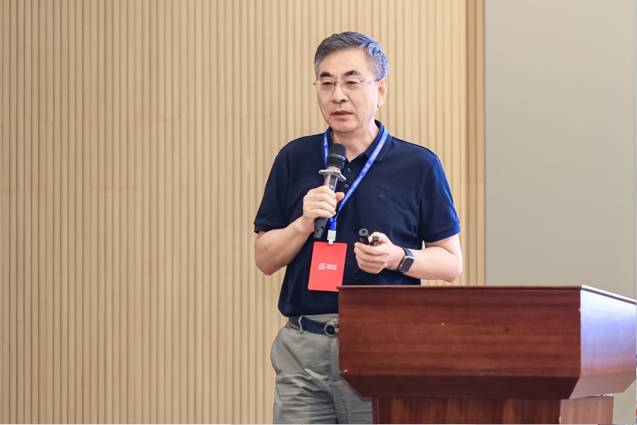
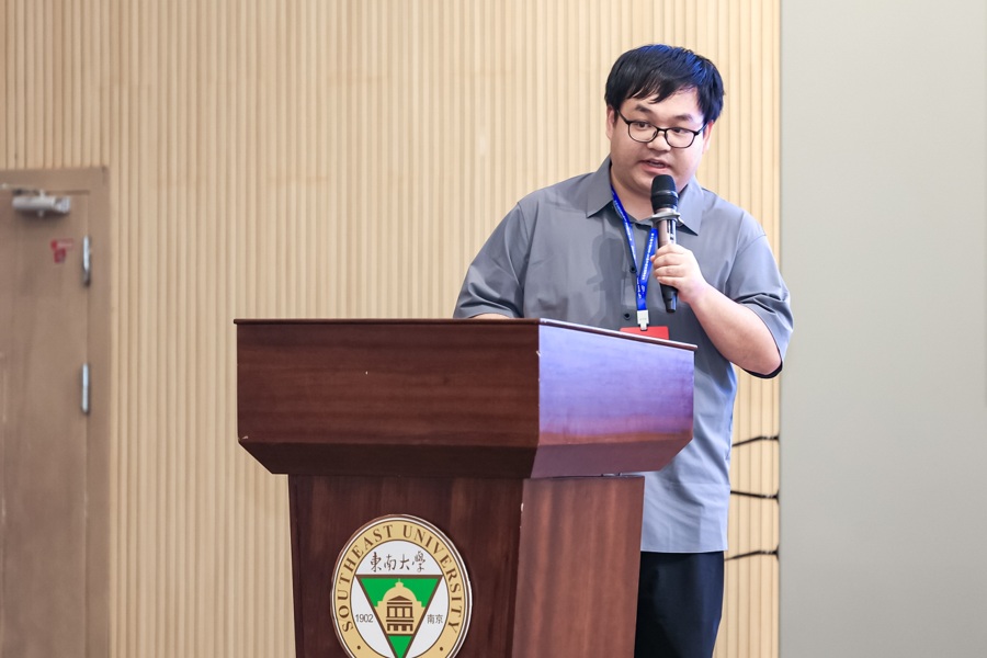
- 马建国(中原工学院)演讲《基于高斯函数的晶体管IV及高阶导数建模》
- 王维波(中国电科第五十五研究所)演讲《AI辅助的异构集成GaN器件建模技术》
- 汪洁(杭州电子科技大学)演讲《面向电路设计的自生成紧凑建模技术》
- 董青杨(北京昂瑞微电子)演讲《手机射频前端与卫星通信的GaN工艺模型挑战》
- 张紫辉(广东工业大学)演讲《GaN半导体器件模拟仿真和研制》
- 王大伟(杭州电子科技大学)演讲《功率器件系统跨层级多物理建模仿真技术研究》
- 毛书漫(电子科技大学长三角研究院)演讲《AI赋能的射频化合物工艺电路协同优化设计》
- 裴轶(苏州能讯高能半导体)演讲《Sub-100nm射频氮化镓工艺平台及模型》
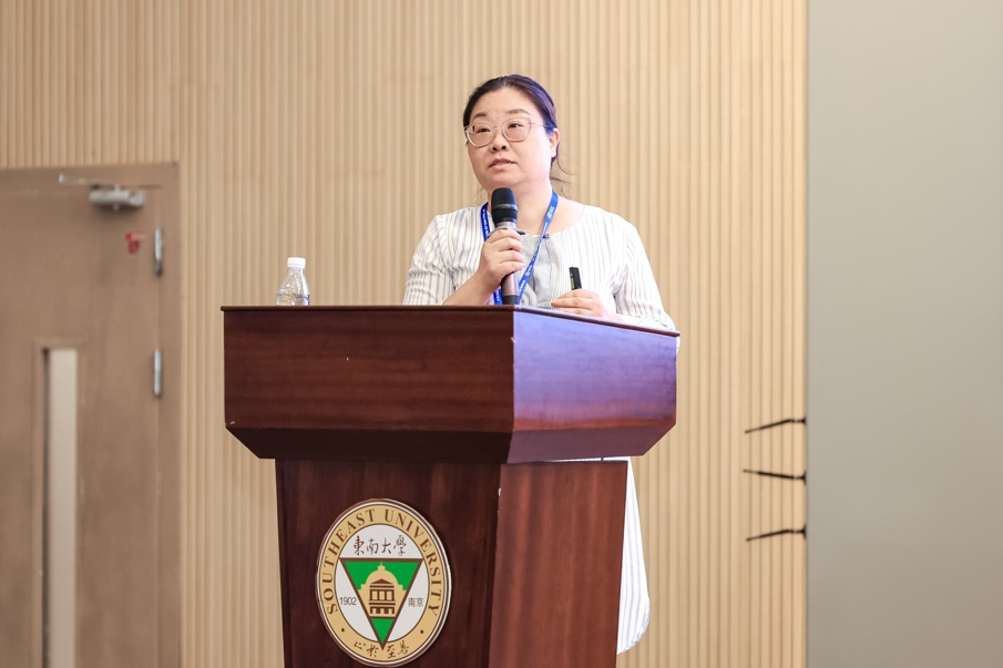
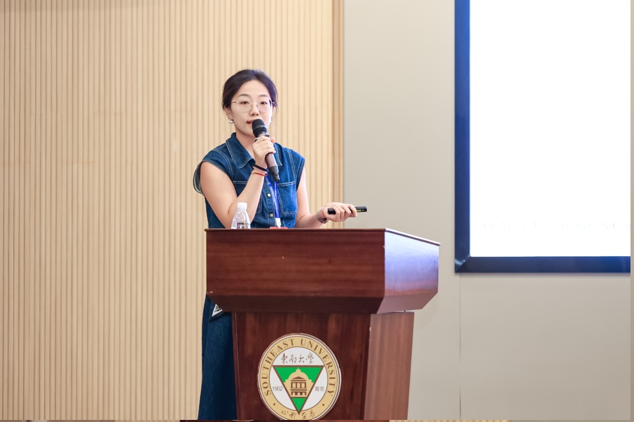
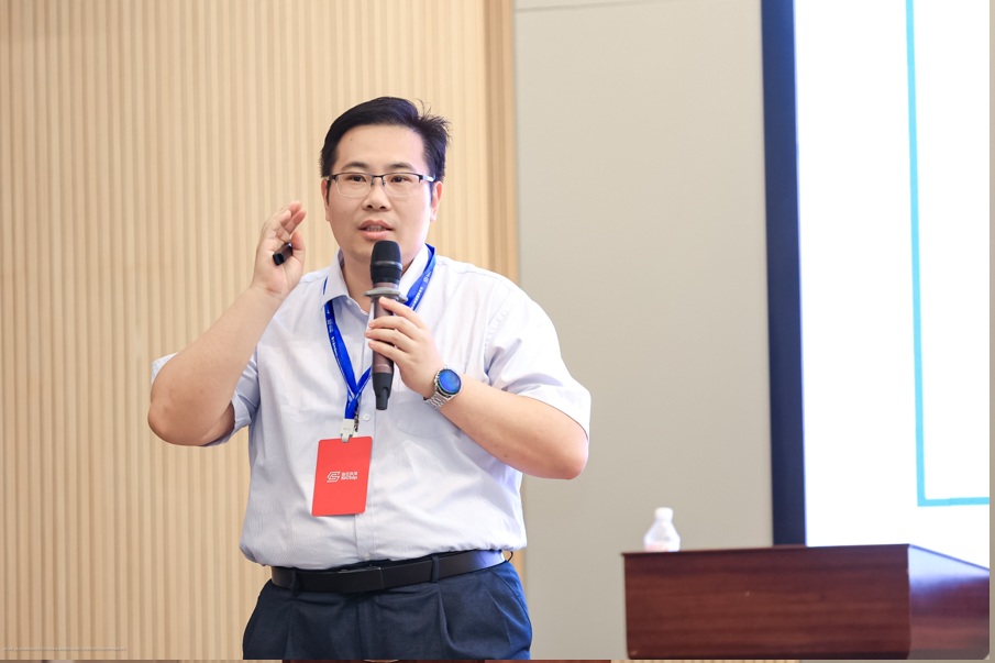
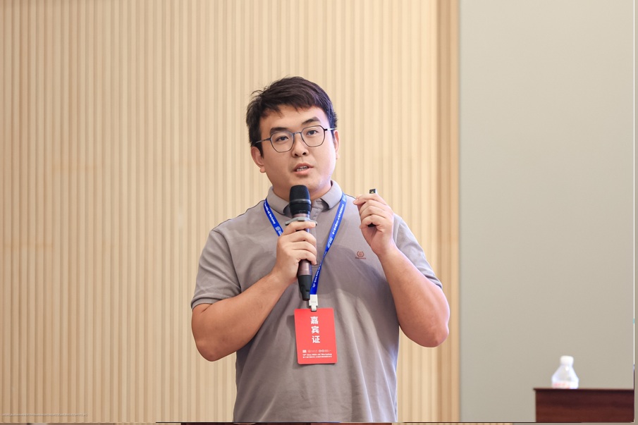
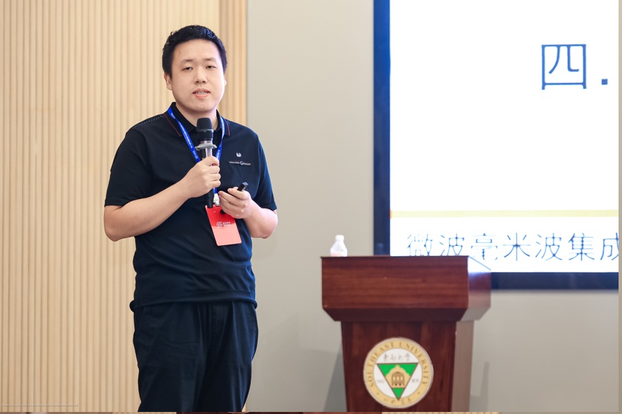
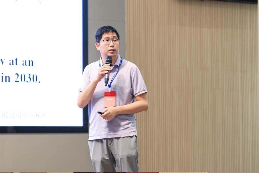
Topic 4: Modeling and simulation of novel devices, such as ultra-low-temperature quantum devices, ultra-wideband memory cells, and non-volatile memory cells. | 专题四:超低温量子器件、超宽带存储单元和非易失性存储单元等新型器件建模和仿真
论坛主席:王成、刘威
- 程然(浙江大学)演讲《面向低温电路应用的特色CMOS工艺和PDK探索》
- 鲍华(上海交通大学)演讲《低温热物性及其对低温CMOS热性能的影响》
- 靳晓笛(北京航空航天大学)演讲《面向InP HEMT超低温的紧凑模型建模》
- 张悦(北京航空航天大学)演讲《自旋存储器件建模与AI赋能设计》
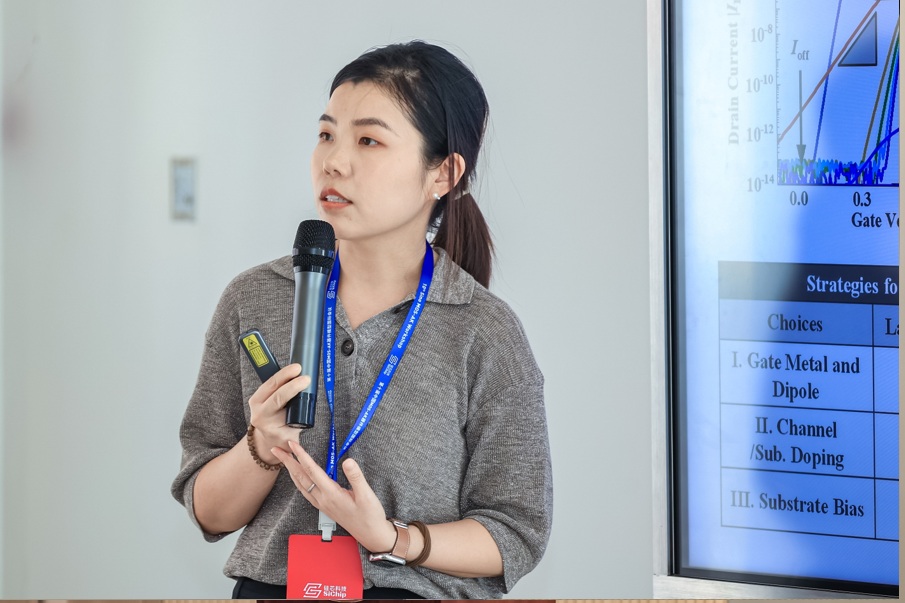
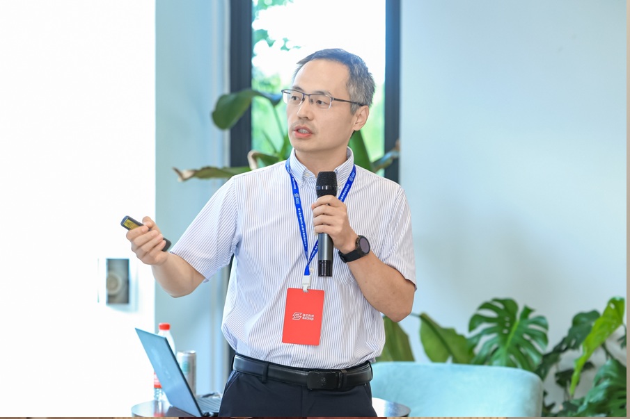
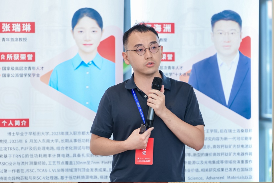
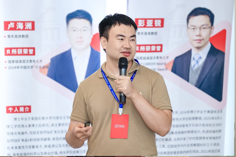
Topic 5: Device Characterization and Testing Techniques, Model Parameter Extraction Techniques, and Interface Strategies between Model Libraries and Foundries | 专题五:器件的表征测试技术、模型参数的提取技术、模型库与晶圆厂的界面策略
论坛主席:靳晓笛、杨廉峰
- 马奕涛(浙江大学)演讲《事件驱动非易失异质集成存算一体芯片与定制化开源PDK》
- 谭小慧(亿方联创)演讲《基于汉擎底座构建智能化PDK QA系统》
- Carol Lin(上海概伦电子)演讲《面向先进CMOS技术的物理信息可靠性与噪声建模——从器件表征到预测性电路仿真》
- 周奕帆(北京航空航天大学)演讲《面向2nm NSFET统计涨落下BSIM-CMG参数提取的DE+SQP混合优化方法及其SRAM应用》
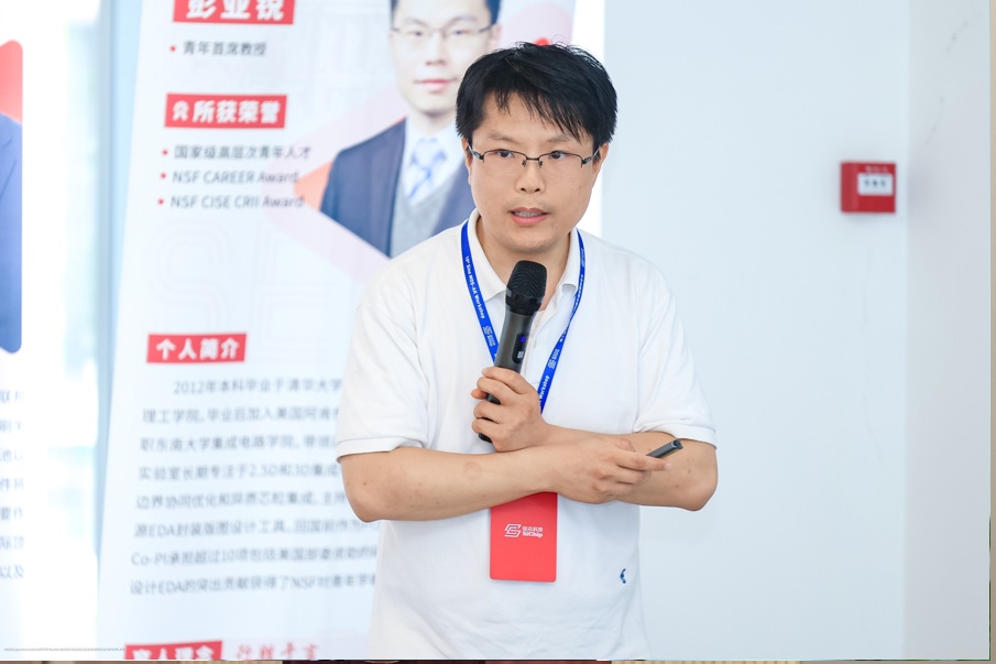
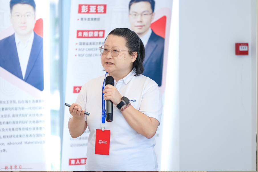
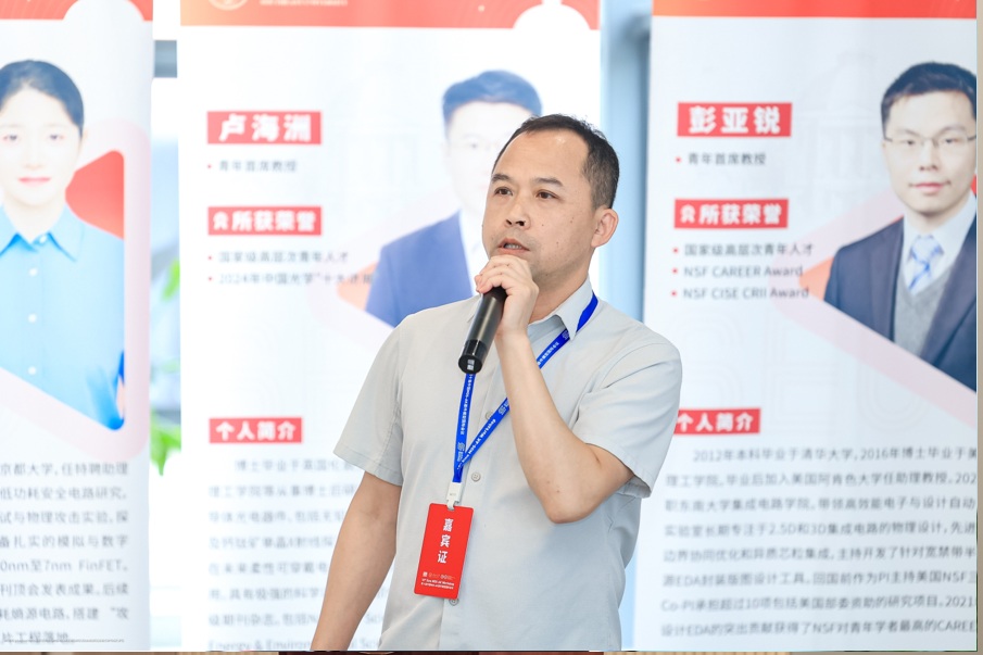
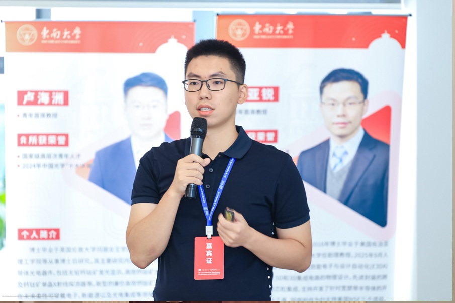
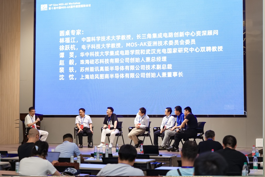
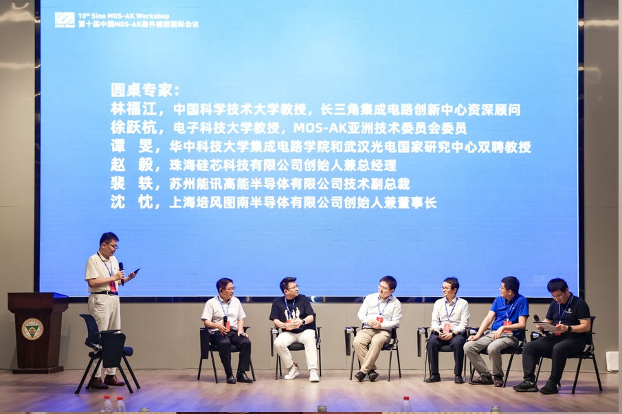
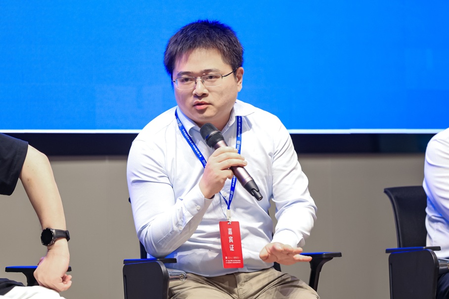
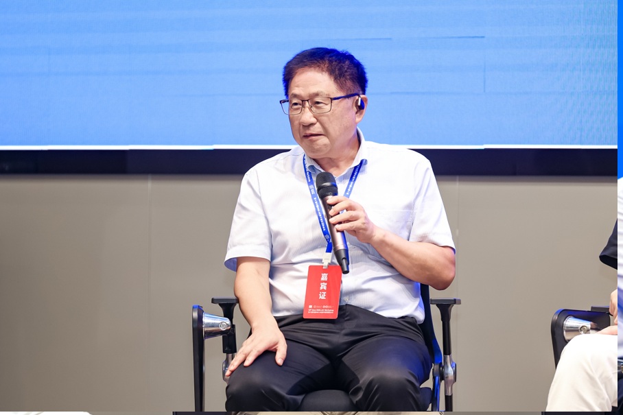
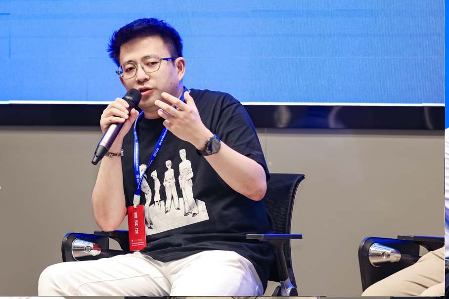
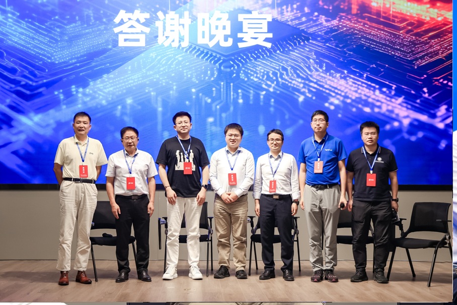
Roundtable Forum: Analyzing Pain Points and Knowledge Gaps in Device Modeling—Collaborative Strategies for Open-Source PDK Model Libraries and Foundry Interfaces | 圆桌论坛:器件建模痛点与认知短板剖析——开源PDK模型库、晶圆厂交互界面协同策略
主持人:李少平
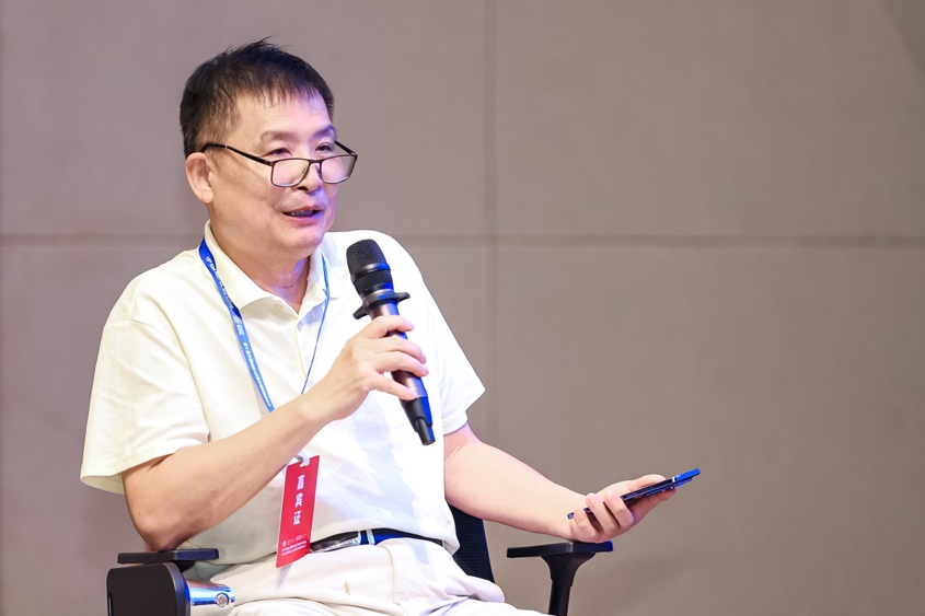
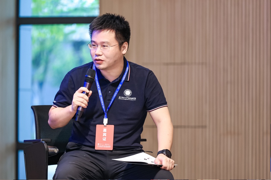
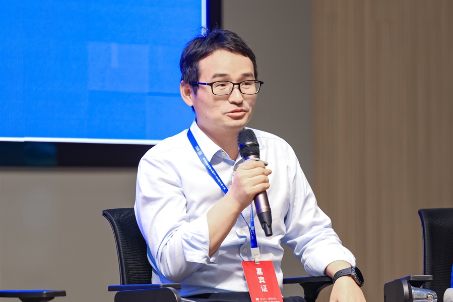
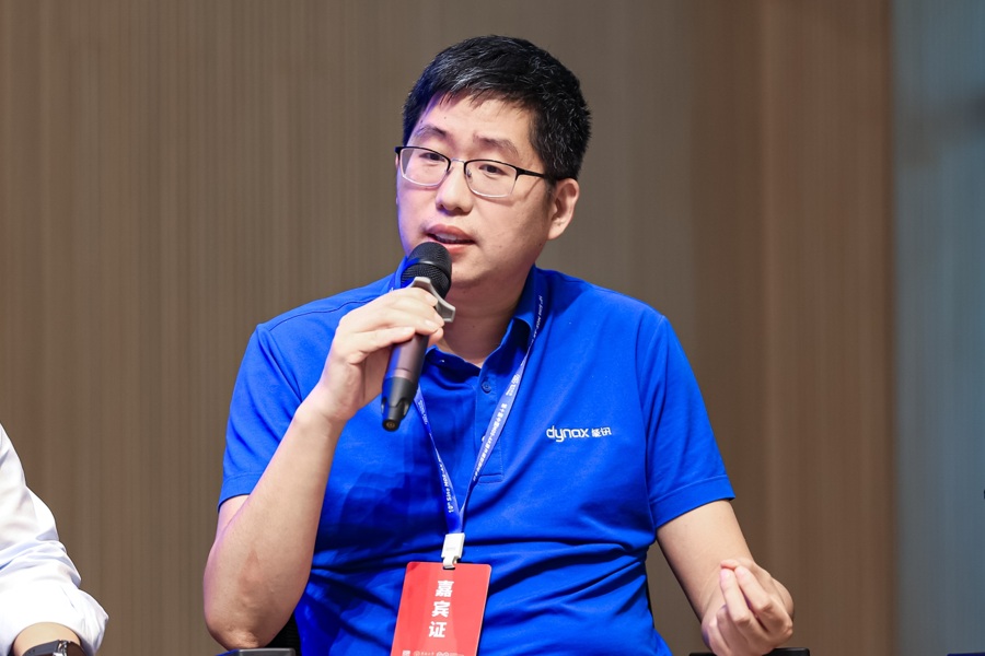
圆桌专家:林福江、孙玲玲、徐跃杭、谭旻、赵毅、裴轶
Key discussion points: the construction of underlying definitions and end-to-end frameworks for device modeling; quantifying the value of modeling within the process-to-chip design chain; the feasibility of implementing open-source PDK model libraries; and differences in technical roadmaps and industry trends regarding device modeling between domestic and international markets.
讨论要点:器件建模底层定义与全流程体系如何构建;建模在工艺—芯片设计链路中的价值如何量化;开源PDK模型库落地可行性;海内外器件建模技术路线与产业趋势差异。
Other event segments | 其他活动环节
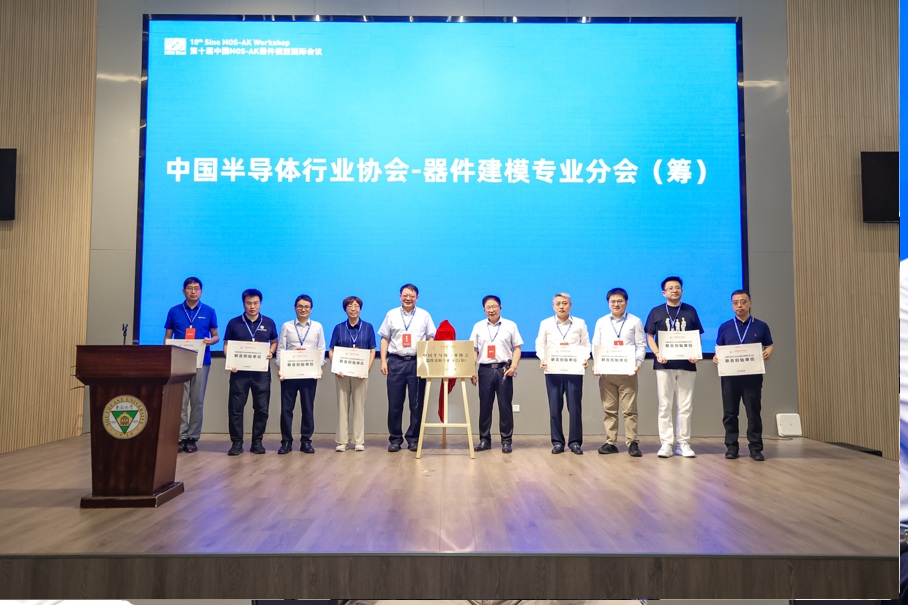
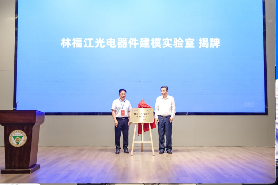
Opening Ceremony and Unveiling: The Semiconductor Device Modeling Branch (Preparatory) of the China Semiconductor Industry Association and the JITRI Lin Fujiang Optoelectronic Device Modeling Laboratory were officially unveiled, and certificates were presented.
开幕式与揭牌:中半协半导体器件建模分会(筹)、JITRI林福江光电器件建模实验室正式揭牌,颁发证书。
Technical Training | 技术培训
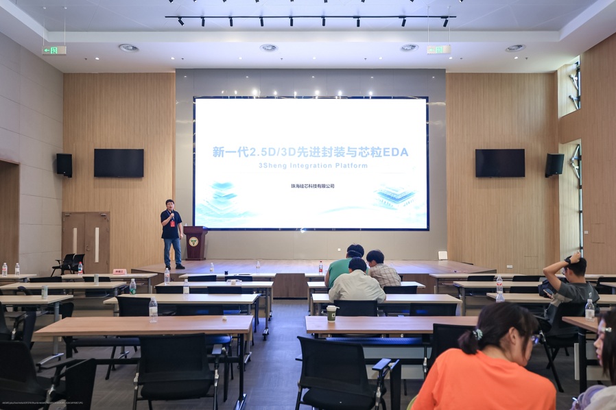
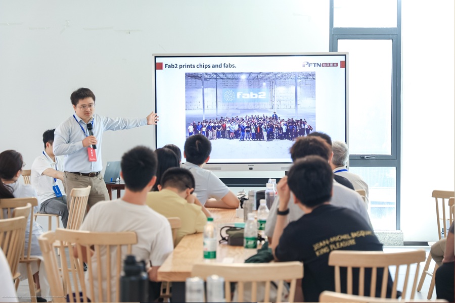
On the afternoon of August 28: Guixin Technology EDA on-site technical training (hands-on demonstration of EDA tools for 2.5D/3D advanced packaging); Peifengtunan Semiconductor EDA on-site training (practical insights into the domestic Mozz TCAD simulation platform at the 55nm CMOS node).
8月28日下午,硅芯科技EDA现场技术培训(2.5D/3D先进封装EDA工具实操演示);培风图南半导体EDA现场培训(55nm CMOS节点国产Mozz TCAD仿真平台实践分享)。
Networking at the dinner | 晚宴交流
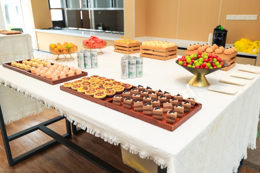
The dinner on the evening of August 27 offers conference guests opportunities for networking and industry matchmaking.
8月27日晚间晚宴,为参会嘉宾提供社交与产业对接机会。
Conference Information | 会议信息
- Dates: August 27–28, 2026
- Venue: Southeast University Wuxi Campus (No. 5 Zhuangyuan Road, Binhu District, Wuxi City, Jiangsu Province)
- Theme: AI-Enabled Device Modeling
- Organizers: Device Modeling Professional Committee of the China Semiconductor Industry Association (Preparatory); Yangtze River Delta Integrated Circuit Industrial Application Technology Innovation Center; IEEE Nanjing Section
- Hosts: School of Integrated Circuits, Southeast University; Asia-Pacific Association of Science and Technology
- 会议时间:2026年8月27日—28日
- 会议地点:东南大学无锡校区(江苏省无锡市滨湖区状元路5号)
- 会议主题:AI赋能器件建模
- 主办单位:中国半导体行业协会器件建模专业分会(筹)、长三角集成电路工业应用技术创新中心、IEEE Nanjing Section
- 承办单位:东南大学集成电路学院、亚太科学技术协会
Leave a Reply